Fueled by the ongoing growth of the gaming market and its insatiable demand for better 3D graphics, NVIDIA® has evolved the GPU into the world’s leading parallel processing engine for many computationally-intensive applications. In addition to rendering highly realistic and immersive 3D games, NVIDIA GPUs also accelerate content creation workflows, high performance computing (HPC) and datacenter applications, and numerous artificial intelligence systems and applications. The new NVIDIA Turing GPU architecture builds on this long-standing GPU leadership.
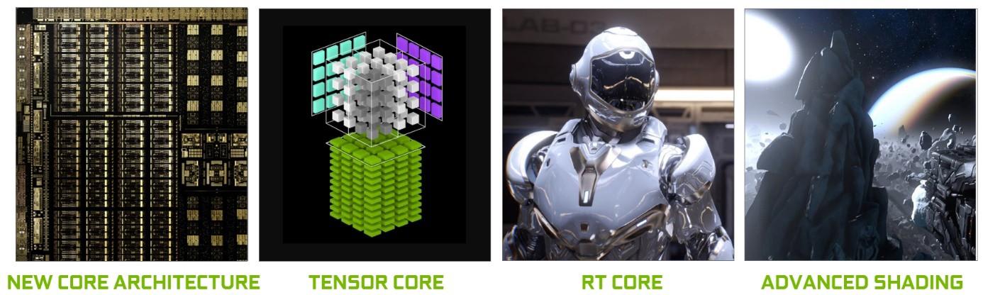
Turing represents the biggest architectural leap forward in over a decade, providing a new core GPU architecture that enables major advances in efficiency and performance for PC gaming, professional graphics applications, and deep learning inferencing.
Using new hardware-based accelerators and a Hybrid Rendering approach, Turing fuses rasterization, real-time ray tracing, AI, and simulation to enable incredible realism in PC games, amazing new effects powered by neural networks, cinematic-quality interactive experiences, and fluid interactivity when creating or navigating complex 3D models.
Within the core architecture, the key enablers for Turing’s significant boost in graphics performance are a new GPU processor (streaming multiprocessor—SM) architecture with improved shader execution efficiency, and a new memory system architecture that includes support for the latest GDDR6 memory technology.
Image processing applications such as the ImageNet Challenge were among the first success stories for deep learning, so it is no surprise that AI has the potential to solve many important problems in graphics. Turing’s Tensor Cores power a suite of new deep learning-based Neural Services that offer stunning graphics effects for games and professional graphics, in addition to providing fast AI inferencing for cloud-based systems.
The long-sought after holy-grail of computer graphics rendering—real-time ray tracing—is now reality in single-GPU systems with the NVIDIA Turing GPU architecture. Turing GPUs introduce new RT Cores, accelerator units that are dedicated to performing ray tracing operations with extraordinary efficiency, eliminating expensive software emulation-based ray tracing approaches of the past. These new units, combined with NVIDIA RTX™ software technology and sophisticated filtering algorithms, enable Turing to deliver real-time ray-traced rendering, including photorealistic objects and environments with physically accurate shadows, reflections, and refractions.
In parallel with Turing’s development, Microsoft announced both the DirectML for AI and DirectX Raytracing (DXR) APIs in early 2018. With the combination of Turing GPU architecture and the new AI and ray tracing APIs from Microsoft, game developers can rapidly deploy real-time AI and ray tracing in their games.
In addition to its groundbreaking AI and ray tracing features, Turing also includes many new advanced shading features that improve performance, enhance image quality, and deliver new levels of geometric complexity.
Turing GPUs also inherit all the enhancements to the NVIDIA CUDA™ platform introduced in the Volta architecture that improve the capability, flexibility, productivity, and portability of compute applications. Features such as independent thread scheduling, hardware-accelerated Multi Process Service (MPS) with address space isolation for multiple applications, and Cooperative Groups are all part of the Turing GPU architecture.
Several of the new NVIDIA GeForce® and NVIDIA Quadro™ GPU products will be powered by Turing GPUs. In this paper we focus on the architecture and capabilities of NVIDIA’s flagship Turing GPU, which is codenamed TU102 and will be shipping in the GeForce RTX 2080 Ti and Quadro RTX 6000. Technical details, including product specifications for TU104 and TU106 Turing GPUs, are located in the appendices.
Figure 1 shows how Turing reinvents graphics with an entirely new architecture that includes enhanced Tensor Cores, new RT Cores, and many new advanced shading features. Turing combines programmable shading, real-time ray tracing, and AI algorithms to deliver incredibly realistic and physically accurate graphics for games and professional applications.
NVIDIA TURING KEY FEATURES
NVIDIA Turing is the world’s most advanced GPU architecture. The high-end TU102 GPU includes
18.6 billion transistors fabricated on TSMC’s 12 nm FFN (FinFET NVIDIA) high-performance manufacturing process.
The GeForce RTX 2080 Ti Founders Edition GPU delivers the following exceptional computational performance:
▶ 14.2 TFLOPS1 of peak single precision (FP32) performance
▶ 28.5 TFLOPS1 of peak half precision (FP16) performance
▶ 14.2 TIPS1 concurrent with FP, through independent integer execution units
▶ 113.8 Tensor TFLOPS1,2
▶ 10 Giga Rays/sec
▶ 78 Tera RTX-OPS
The Quadro RTX 6000 provides superior computational performance designed for professional workflows:
▶ 16.3 TFLOPS1 of peak single precision (FP32) performance
▶ 32.6 TFLOPS1 of peak half precision (FP16) performance
▶ 16.3 TIPS1 concurrent with FP, through independent integer execution units
▶ 130.5 Tensor TFLOPS1,2
▶ 10 Giga Rays/sec
▶ 84 Tera RTX-OPS
1Based on GPU Boost clock. 2FP16 matrix math with FP16 accumulation.
The following section describes Turing’s major new innovations in summary format. More detailed descriptions of each area are provided throughout this whitepaper.
New Streaming Multiprocessor (SM)
Turing introduces a new processor architecture, the Turing SM, that delivers a dramatic boost in shading efficiency, achieving 50% improvement in delivered performance per CUDA Core compared to the Pascal generation. These improvements are enabled by two key architectural changes. First, the Turing SM adds a new independent integer datapath that can execute instructions concurrently with the floating-point math datapath. In previous generations, executing these instructions would have blocked floating-point instructions from issuing. Second, the SM memory path has been redesigned to unify shared memory, texture caching, and memory load caching into one unit. This translates to 2x more bandwidth and more than 2x more capacity available for L1 cache for common workloads.
![]() Turing Tensor Cores
Turing Tensor Cores
Tensor Cores are specialized execution units designed specifically for performing the tensor / matrix operations that are the core compute function used in Deep Learning. Similar to Volta Tensor Cores, the Turing Tensor Cores provide tremendous speed-ups for matrix computations at the heart of deep learning neural network training and inferencing operations. Turing GPUs include a new version of the Tensor Core design that has been enhanced for inferencing. Turing Tensor Cores add new INT8 and INT4 precision modes for inferencing workloads that can tolerate quantization and don’t require FP16 precision. Turing Tensor Cores bring new deep learning- based AI capabilities to GeForce gaming PCs and Quadro-based workstations for the first time. A new technique called Deep Learning Super Sampling (DLSS) is powered by Tensor Cores. DLSS leverages a deep neural network to extract multidimensional features of the rendered scene and intelligently combine details from multiple frames to construct a high-quality final image. DLSS uses fewer input samples than traditional techniques such as TAA, while avoiding the algorithmic difficulties such techniques face with transparency and other complex scene elements.
Real-Time Ray Tracing Acceleration
Turing introduces real-time ray tracing that enables a single GPU to render visually realistic 3D games and complex professional models with physically accurate shadows, reflections, and refractions. Turing’s new RT Cores accelerate ray tracing and are leveraged by systems and interfaces such as NVIDIA’s RTX ray tracing technology, and APIs such as Microsoft DXR, NVIDIA OptiX™, and Vulkan ray tracing to deliver a real-time ray tracing experience.
New Shading Advancements
Mesh Shading
Mesh shading advances NVIDIA’s geometry processing architecture by offering a new shader model for the vertex, tessellation, and geometry shading stages of the graphics pipeline, supporting more flexible and efficient approaches for computation of geometry. This more flexible model makes it possible, for example, to support an order of magnitude more objects per scene, by moving the key performance bottleneck of object list processing off of the CPU and into highly parallel GPU mesh shading programs. Mesh shading also enables new algorithms for advanced geometric synthesis and object LOD management.
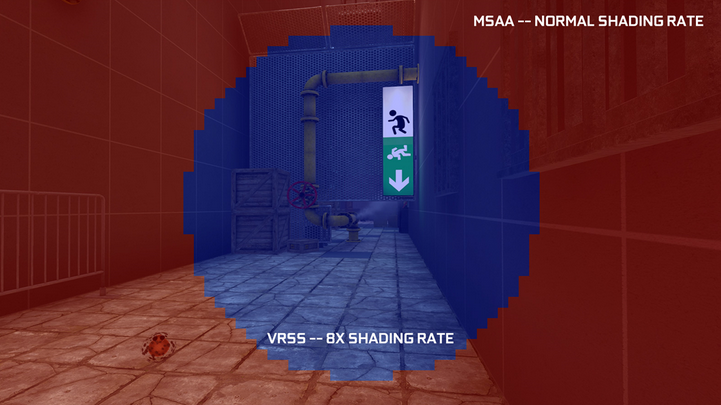
Variable Rate Shading (VRS)
VRS allows developers to control shading rate dynamically, shading as little as once per sixteen pixels or as often as eight times per pixel. The application specifies shading rate using a combination of a shading-rate surface and a per-primitive (triangle) value. VRS is a very powerful tool that allows developers to shade more efficiently, reducing work in regions of the screen where full resolution shading would not give any visible image quality benefit, and therefore improving frame rate. Several classes of VRS-based algorithms have already been identified, which can vary shading work based on content level of detail (Content Adaptive Shading), rate of content motion (Motion Adaptive Shading), and for VR applications, lens resolution and eye position (Foveated Rendering).
Texture-Space Shading
With texture-space shading, objects are shaded in a private coordinate space (a texture space) that is saved to memory, and pixel shaders sample from that space rather than evaluating results directly. With the ability to cache shading results in memory and reuse/resample them, developers can eliminate duplicate shading work or use different sampling approaches that improve quality.
Multi-View Rendering (MVR)
MVR powerfully extends Pascal’s Single Pass Stereo (SPS). While SPS allowed rendering of two views that were common except for an X offset, MVR allows rendering of multiple views in a single pass even if the views are based on totally different origin positions or view directions. Access is via a simple programming model in which the compiler automatically factors out view independent code, while identifying view-dependent attributes for optimal execution.
Deep Learning Features for Graphics
NVIDIA NGX™ is the new deep learning-based neural graphics framework of NVIDIA RTX Technology. NVIDIA NGX utilizes deep neural networks (DNNs) and set of “Neural Services” to perform AI-based functions that accelerate and enhance graphics, rendering, and other client- side applications. NGX employs the Turing Tensor Cores for deep learning-based operations and accelerates delivery of NVIDIA deep learning research directly to the end-user. Features include ultra-high quality NGX DLSS (Deep Learning Super-Sampling), AI InPainting content-aware image replacement, AI Slow-Mo very high-quality and smooth slow motion, and AI Super Rez smart resolution resizing.
Deep Learning Features for Inference
Turing GPUs deliver exceptional inference performance. The Turing Tensor Cores, along with continual improvements in TensorRT (NVIDIA’s run-time inferencing framework), CUDA, and CuDNN libraries, enable Turing GPUs to deliver outstanding performance for inferencing applications. Turing Tensor Cores also add support for fast INT8 matrix operations to significantly accelerate inference throughput with minimal loss in accuracy. New low-precision INT4 matrix operations are now possible with Turing Tensor Cores and will enable research and development into sub 8-bit neural networks.
GDDR6 High-Performance Memory Subsystem
Turing is the first GPU architecture to support GDDR6 memory. GDDR6 is the next big advance in high-bandwidth GDDR DRAM memory design. GDDR6 memory interface circuits in Turing GPUs have been completely redesigned for speed, power efficiency and noise reduction, achieving 14 Gbps transfer rates at 20% improved power efficiency compared to GDDR5X memory used in Pascal GPUs.
Second-Generation NVIDIA NVLink
Turing TU102 and TU104 GPUs incorporate NVIDIA’s NVLink™ high-speed interconnect to provide dependable, high bandwidth and low latency connectivity between pairs of Turing GPUs. With up to 100GB/sec of bidirectional bandwidth, NVLink makes it possible for customized workloads to efficiently split across two GPUs and share memory capacity. For gaming workloads, NVLink’s increased bandwidth and dedicated inter-GPU channel enables new possibilities for SLI, such as new modes or higher resolution display configurations. For large memory workloads, including professional ray tracing applications, scene data can be split across the frame buffer of both GPUs, offering up to 96 GB of shared frame buffer memory (two 48 GB Quadro RTX 8000 GPUs), and memory requests are automatically routed by hardware to the correct GPU based on the location of the memory allocation.
USB-C and VirtualLink
Turing GPUs include hardware support for USB Type-C™ and VirtualLink™. (In preparation for the emerging VirtualLink standard, Turing GPUs have implemented hardware support according to the VirtualLink Advance Overview. To learn more about VirtualLink, refer to http://www.virtuallink.org). VirtualLink is a new open industry standard being developed to meet the power, display, and bandwidth demands of next-generation VR headsets through a single USB-C connector. In addition to easing the setup hassles present in today’s VR headsets, VirtualLink will bring VR to more devices.
![]() Turing Architecture In-depth
Turing Architecture In-depth
The Turing TU102 GPU is the highest performing GPU of the Turing GPU line and the focus of this section. The TU104 and TU106 GPUs utilize the same basic architecture as TU102, scaled down to different degrees for different usage models and market segments. Details of TU104 and TU106 chip architectures and target usages/markets are provided in the full Turing Architecture White Paper.
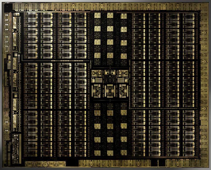
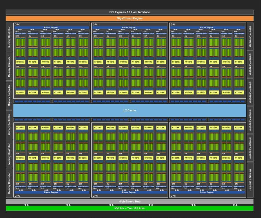
TURING TU102 GPU
The TU102 GPU includes six Graphics Processing Clusters (GPCs), 36 Texture Processing Clusters (TPCs), and 72 Streaming Multiprocessors (SMs). (See Figure 2 for an illustration of the TU102 full GPU with 72 SM units.) Each GPC includes a dedicated raster engine and six TPCs, with each TPC including two SMs. Each SM contains 64 CUDA Cores, eight Tensor Cores, a 256 KB register file, four texture units, and 96 KB of L1/shared memory which can be configured for various capacities depending on the compute or graphics workloads.
Ray tracing acceleration is performed by a new RT Core processing engine within each SM (RT Core and ray tracing features are discussed in more depth in the full NVIDIA Turing Architecture White Paper).
The full implementation of the TU102 GPU includes the following:
▶ 4,608 CUDA Cores
▶ 72 RT Cores
▶ 576 Tensor Cores
▶ 288 texture units
▶ 12 32-bit GDDR6 memory controllers (384-bits total).
Tied to each memory controller are eight ROP units and 512 KB of L2 cache. The full TU102 GPU consists of 96 ROP units and 6144 KB of L2 cache. See the Turing TU102 GPU in Figure 3. Table 1 compares the GPU features of the Pascal GP102 to the Turing TU102.
Note: The TU102 GPU also features 144 FP64 units (two per SM), which are not depicted in this diagram. The FP64 TFLOP rate is 1/32nd the TFLOP rate of FP32 operations. The small number of FP64 hardware units are included to ensure any programs with FP64 code operates correctly.
| GPU Features | GTX 1080Ti | RTX 2080 Ti | Quadro 6000 | Quadro RTX 6000 |
| Architecture | Pascal | Turing | Pascal | Turing |
| GPCs | 6 | 6 | 6 | 6 |
| TPCs | 28 | 34 | 30 | 36 |
| SMs | 28 | 68 | 30 | 72 |
| CUDA Cores / SM | 128 | 64 | 128 | 64 |
| CUDA Cores / GPU | 3584 | 4352 | 3840 | 4608 |
| Tensor Cores / SM | NA | 8 | NA | 8 |
| Tensor Cores / GPU | NA | 544 | NA | 576 |
| RT Cores | NA | 68 | NA | 72 |
| GPU Base Clock MHz (Reference / Founders Edition) | 1480 / 1480 | 1350 / 1350 | 1506 | 1455 |
| GPU Boost Clock MHz (Reference / Founders Edition) | 1582 / 1582 | 1545 / 1635 | 1645 | 1770 |
| RTX-OPS (Tera-OPS)
(Reference / Founders Edition) |
11.3 / 11.3 | 76 / 78 | NA | 84 |
| Rays Cast (Giga Rays/sec) (Reference / Founders Edition) | 1.1 / 1.1 | 10 / 10 | NA | 10 |
| Peak FP32 TFLOPS✱
(Reference/Founders Edition) |
11.3 / 11.3 | 13.4 / 14.2 | 12.6 | 16.3 |
| Peak INT32 TIPS✱
(Reference/Founders Edition) |
NA | 13.4 / 14.2 | NA | 16.3 |
| Peak FP16 TFLOPS✱
(Reference/Founders Edition) |
NA | 26.9 / 28.5 | NA | 32.6 |
| Peak FP16 Tensor TFLOPS with FP16 Accumulate✱ (Reference/Founders Edition) | NA | 107.6 / 113.8 | NA | 130.5 |
| Peak FP16 Tensor TFLOPS with FP32 Accumulate✱ (Reference/Founders Edition) | NA | 53.8 / 56.9 | NA | 130.5 |
| Peak INT8 Tensor TOPS✱ (Reference/Founders Edition) | NA | 215.2 / 227.7 | NA | 261.0 |
| Peak INT4 Tensor TOPS✱
(Reference/Founders Edition) |
NA | 430.3 / 455.4 | NA | 522.0 |
| Frame Buffer Memory Size and Type | 11264 MB GDDR5X | 11264 MB GDDR6 | 24576 MB GDDR5X | 24576 MB GDDR6 |
| Memory Interface | 352-bit | 352-bit | 384-bit | 384-bit |
| Memory Clock (Data Rate) | 11 Gbps | 14 Gbps | 9 Gbps | 14 Gbps |
| Memory Bandwidth (GB/sec) | 484 | 616 | 432 | 672 |
| ROPs | 88 | 88 | 96 | 96 |
| Texture Units | 224 | 272 | 240 | 288 |
| Texel Fill-rate (Gigatexels/sec) | 354.4 / 354.4 | 420.2 / 444.7 | 395 | 510 |
| L2 Cache Size | 2816 KB | 5632 KB | 3072 KB | 6144 KB |
| Register File Size/SM | 256 KB | 256 KB | 256 KB | 256 KB |
| Register File Size/GPU | 7168 KB | 17408 KB | 7680 KB | 18432 KB |
| TDP★
(Reference/Founders Edition) |
250 / 250 W | 250 / 260 W | 250 W | 260 W |
| Transistor Count | 12 Billion | 18.6 Billion | 12 Billion | 18.6 Billion |
| Die Size | 471 | 754 | 471 | 754 |
| Manufacturing Process | 16 nm | 12 nm FFN | 16 nm | 12 nm FFN |
As GPU-accelerated computing has become more popular, systems with multiple GPUs are increasingly being deployed in servers, workstations, and supercomputers. The TU102 and TU104 GPUs include the second generation of NVIDIA’s NVLink™ high-speed interconnect, originally designed into the Volta GV100 GPU, providing high-speed multi-GPU connectivity for SLI and other multi-GPU use cases. NVLink permits each GPU to directly access memory of other connected GPUs, providing much faster GPU-to-GPU communications, and allows combining memory from multiple GPUs to support much larger datasets and faster in-memory computations.
TU102 includes two NVLink x8 links each capable of delivering up to 25 Gigabytes/second in each direction, for a total aggregate bidirectional bandwidth of 100 Gigabytes/second.

TURING STREAMING MULTIPROCESSOR (SM) ARCHITECTURE
The Turing architecture features a new SM design that incorporates many of the features introduced in our Volta GV100 SM architecture. Two SMs are included per TPC, and each SM has a total of 64 FP32 Cores and 64 INT32 Cores. In comparison, the Pascal GP10x GPUs have one SM per TPC and 128 FP32 Cores per SM. The Turing SM supports concurrent execution of FP32 and INT32 operations (more details below), independent thread scheduling similar to the Volta GV100 GPU. Each Turing SM also includes eight mixed-precision Turing Tensor Cores, which are described in more detail in the Turing Tensor Cores section below , and one RT Core, whose functionality is described in the Turing Ray Tracing Technology below. See Figure 4 for an illustration of the Turing TU102, TU104, and TU106 SM.
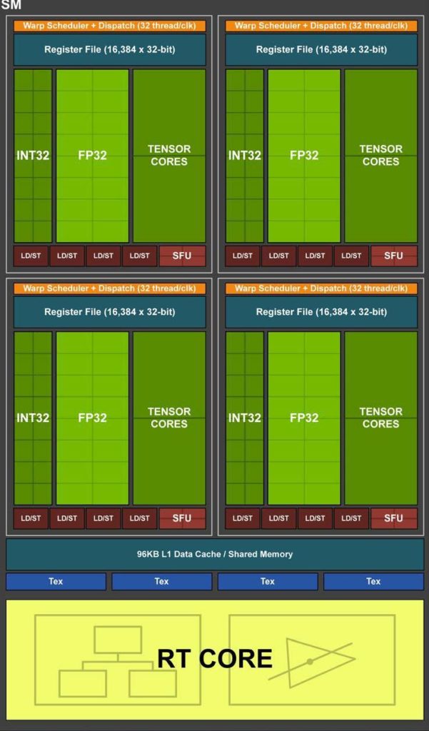
The Turing SM is partitioned into four processing blocks, each with 16 FP32 Cores, 16 INT32 Cores, two Tensor Cores, one warp scheduler, and one dispatch unit. Each block includes a new L0 instruction cache and a 64 KB register file. The four processing blocks share a combined 96 KB L1 data cache/shared memory. Traditional graphics workloads partition the 96 KB L1/shared memory as 64 KB of dedicated graphics shader RAM and 32 KB for texture cache and register file spill area. Compute workloads can divide the 96 KB into 32 KB shared memory and 64 KB L1 cache, or 64 KB shared memory and 32 KB L1 cache.
Turing implements a major revamping of the core execution datapaths. Modern shader workloads typically have a mix of FP arithmetic instructions such as FADD or FMAD with simpler instructions such as integer adds for addressing and fetching data, floating point compare or min/max for processing results, etc. In previous shader architectures, the floating-point math datapath sits idle whenever one of these non-FP-math instructions runs. Turing adds a second parallel execution unit next to every CUDA core that executes these instructions in parallel with floating point math.
Figure 5 shows that the mix of integer pipe versus floating point instructions varies, but across several modern applications, we typically see about 36 additional integer pipe instructions for every 100 floating point instructions. Moving these instructions to a separate pipe translates to an effective 36% additional throughput possible for floating point.
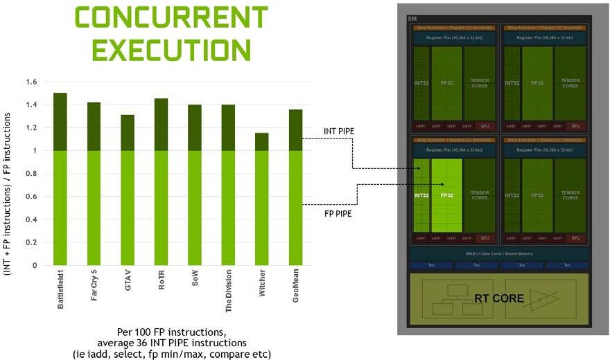
Profiling many workloads shows an average of 36 integer operations for every 100 floating point operations.
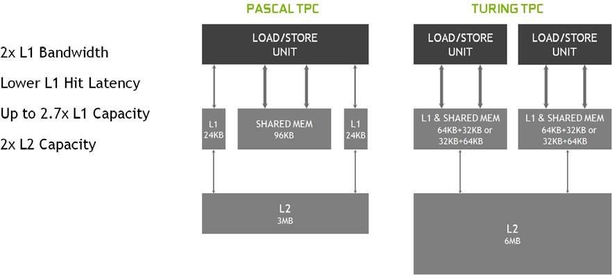
Turing’s SM also introduces a new unified architecture for shared memory, L1, and texture caching. This unified design allows the L1 cache to leverage resources, increasing its hit bandwidth by 2x per TPC compared to Pascal, and allows it to be reconfigured to grow larger when shared memory allocations are not using all the shared memory capacity. The Turing L1 can be as large as 64 KB in size, combined with a 32 KB per SM shared memory allocation, or it can reduce to 32 KB, allowing 64 KB of allocation to be used for shared memory. Turing’s L2 cache capacity has also been increased.
Figure 6 shows how the new combined L1 data cache and shared memory subsystem of the Turing SM significantly improves performance while also simplifying programming and reducing the tuning required to attain at or near-peak application performance. Combining the L1 data cache with the shared memory reduces latency and provides higher bandwidth than the L1 cache implementation used previously in Pascal GPUs.
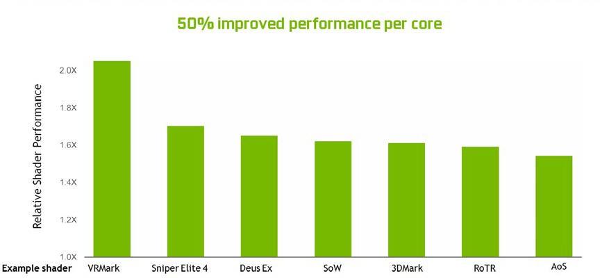
Overall, the changes in SM enable Turing to achieve 50% improvement in delivered performance per CUDA core. Figure 7 shows the results across a set of shader workloads from current gaming applications.
Turing Tensor Cores
Turing GPUs include an enhanced version of the Tensor Cores first introduced in the Volta GV100 GPU. The Turing Tensor Core design adds INT8 and INT4 precision modes for inferencing workloads that can tolerate quantization. FP16 is also fully supported for workloads that require higher precision.
The introduction of Tensor Cores into Turing-based GeForce gaming GPUs makes it possible to bring real-time deep learning to gaming applications for the first time. Turing Tensor Cores accelerate the AI-based features of NVIDIA NGX Neural Services that enhance graphics, rendering, and other types of client-side applications. Examples of NGX AI features include Deep Learning Super Sampling (DLSS), AI InPainting, AI Super Rez, and AI Slow-Mo. More details on DLSS can be found later in this post. You can find additional information on other NGX functionality in the full NVIDIA Turing Architecture White Paper.
Turing Tensor Cores accelerate the matrix-matrix multiplication at the heart of neural network training and inferencing functions. Turing Tensor Cores particularly excel at inference computations, in which useful and relevant information can be inferred and delivered by a trained deep neural network (DNN) based on a given input. Examples of inference include identifying images of friends in Facebook photos, identifying and classifying different types of automobiles, pedestrians, and road hazards in self-driving cars, translating human speech in real- time, and creating personalized user recommendations in online retail and social media systems.
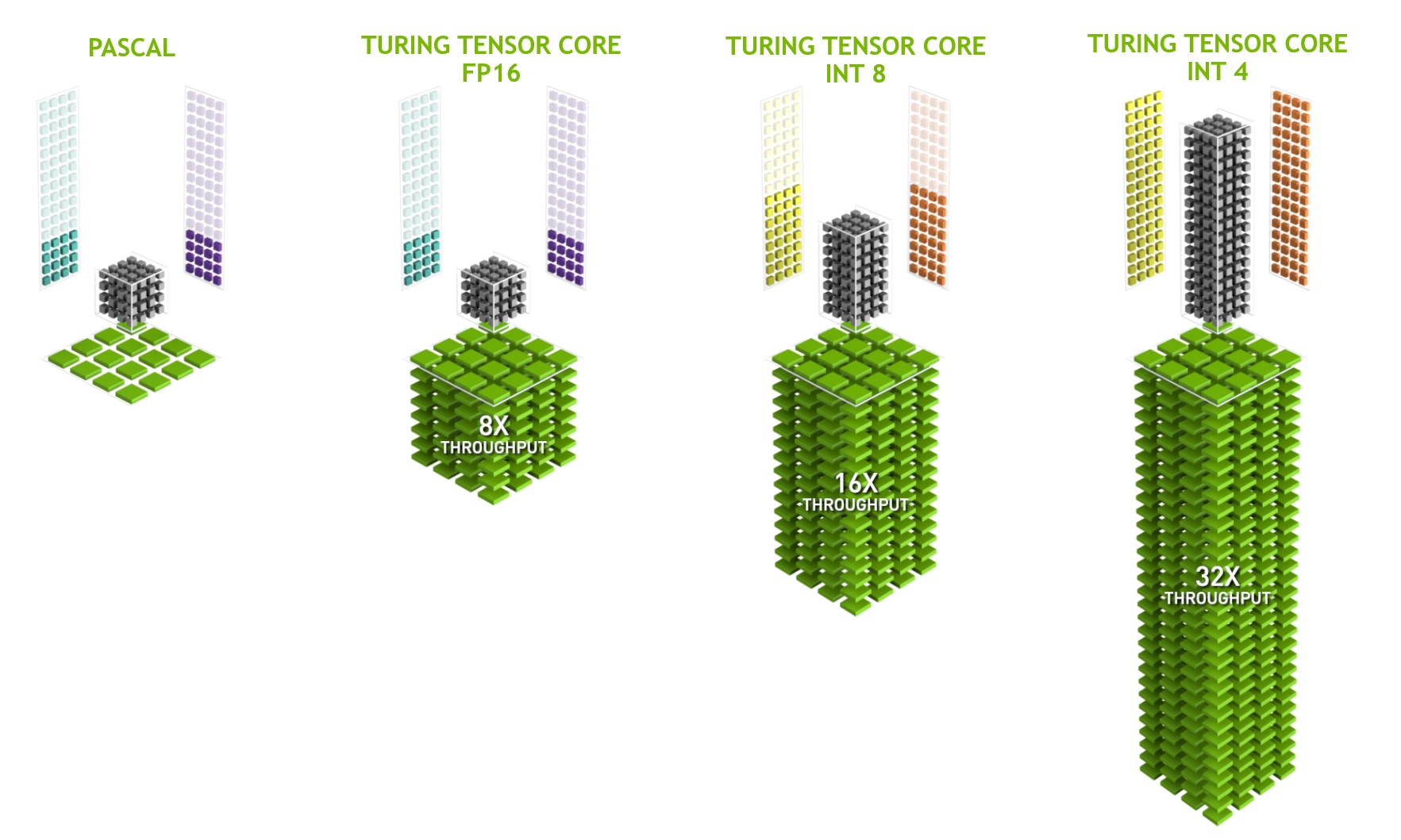
A TU102 GPU contains 576 Tensor Cores: eight per SM and two per each processing block within an SM. Each Tensor Core can perform up to 64 floating point fused multiply-add (FMA) operations per clock using FP16 inputs. Eight Tensor Cores in an SM perform a total of 512 FP16 multiply and accumulate operations per clock, or 1024 total FP operations per clock. The new INT8 precision mode works at double this rate, or 2048 integer operations per clock.
Turing Tensor Cores provide significant speedups to matrix operations and are used for both deep learning training and inference operations in addition to new neural graphics functions. For more information on basic Tensor Core operational details refer to the NVIDIA Tesla V100 GPU Architecture Whitepaper.
TURING OPTIMIZED FOR DATACENTER APPLICATIONS
In addition to bringing revolutionary new features for high-end gaming and professional graphics, Turing delivers exceptional performance and energy efficiency for the next generation of Tesla® GPUs. NVIDIA’s current generation of Pascal-based GPUs used in datacenters for inferencing applications already deliver up to 10 times higher performance and 25 times higher energy efficiency than CPU-based servers. Powered by the Turing Tensor Cores, the next generation of Turing-based Tesla GPUs will deliver even higher inferencing performance and energy efficiency in data centers. Turing-based Tesla GPUs optimized to operate under 70 Watts will deliver significant efficiency and performance boost to hyperscale data centers.
Turing GPU architecture, in addition to the Turing Tensor Cores, includes several features to improve performance of data center applications. Some of the key features are:
Enhanced Video Engine
Compared to prior generation Pascal and Volta GPU architectures, Turing supports additional video decode formats such as HEVC 4:4:4 (8/10/12 bit), and VP9 (10/12 bit). The enhanced video engine in Turing is capable of decoding significantly higher number of concurrent video streams than equivalent Pascal based Tesla GPUs. (See the Video and Display Engine section below.)
Turing Multi-Process Service
Turing GPU architecture inherits the enhanced Multi-Process Service (MPS) feature first introduced in the Volta architecture. Compared to Pascal-based Tesla GPUs, MPS on Turing- based Tesla boards improve inference performance for small batch sizes, reduce launch latency, improve Quality of Service, and can service higher numbers of concurrent client requests.
Higher memory bandwidth and larger memory size
Upcoming Turing-based Tesla boards have larger memory capacity and higher memory bandwidth than prior generation Pascal-based Tesla boards that target similar server segments, delivering greater user density for Virtual Desktop Infrastructure (VDI) applications.
TURING MEMORY ARCHITECTURE AND DISPLAY FEATURES
This section dives deeper into key new memory hierarchy and display subsystem features of the Turing architecture.
Memory subsystem performance is crucial to application acceleration. Turing improves main memory, cache memory, and compression architectures to increase memory bandwidth and reduce access latency. Improved and enhanced GPU compute features help accelerate both games and many computationally intensive applications and algorithms. New display and video encode/decode features support higher resolution and HDR-capable displays, more advanced VR displays, increasing video streaming requirements in the datacenter, 8K video production, and other video-related applications. The following features are discussed in detail:
GDDR6 Memory Subsystem
As display resolutions continue to increase and shader functionality and rendering techniques become more complex, memory bandwidth and size play a larger role in GPU performance. To maintain the highest possible frame rates and computational speed, the GPU not only needs more memory bandwidth, it also needs a large pool of memory to draw from to deliver sustained performance.
NVIDIA worked closely with the DRAM industry to develop the world’s first GPUs that use HBM2 and GDDR5X memories. Now Turing is the first GPU architecture to utilize GDDR6 memory.
GDDR6 is the next big advance in high-bandwidth GDDR DRAM memory design. Enhanced with many high-speed SerDes and RF techniques, GDDR6 memory interface circuits in Turing GPUs have been completely redesigned for speed, power efficiency, and noise reduction. This new interface design comes with many new circuit and signal training improvements that minimize noise and variations due to process, temperature, and supply voltage. Extensive clock gating was used to minimize power consumption during periods of lower utilization, resulting in significant overall power efficiency improvement. Turing’s GDDR6 memory subsystem delivers 14 Gbps signaling rates and 20% power efficiency improvement over GDDR5X memory used in Pascal GPUs.
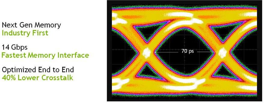
Achieving this speed increase requires end-to-end optimizations. Using extensive signal and power integrity simulations, NVIDIA carefully crafted Turing’s package and board designs to meet the higher speed requirements. An example is a 40% reduction in signal crosstalk, which is one of the most severe impairments in large memory systems.
To realize speeds of 14 Gbps, every aspect of the memory subsystem was carefully crafted to meet the demanding standards that are required for such high frequency operation. Every signal in the design was carefully optimized to provide the cleanest memory interface signaling as possible (see Figure 9).
L2 Cache and ROPs
Turing GPUs add larger and faster L2 caches in addition to the new GDDR6 memory subsystem. The TU102 GPU ships with 6 MB of L2 cache, double the 3 MB of L2 cache that was offered in the prior generation GP102 GPU used in the TITAN Xp. TU102 also provides significantly higher L2 cache bandwidth than GP102.
Like prior generation NVIDIA GPUs, each ROP partition in Turing contains eight ROP units and each unit can process a single-color sample. A full TU102 chip contains 12 ROP partitions for a total of 96 ROPs.
Turing Memory Compression
NVIDIA GPUs utilize several lossless memory compression techniques to reduce memory bandwidth demands as data is written out to frame buffer memory. The GPU’s compression engine has a variety of different algorithms which determine the most efficient way to compress the data based on its characteristics. This reduces the amount of data written out to memory and transferred from memory to the L2 cache and reduces the amount of data transferred between clients (such as the texture unit) and the frame buffer. Turing adds further improvements to Pascal’s state-of-the-art memory compression algorithms, offering a further boost in effective bandwidth beyond the raw data transfer rate increases of GDDR6. As shown in Figure 10, the combination of raw bandwidth increases, and traffic reduction translates to a 50% increase in effective bandwidth on Turing compared to Pascal, which is critical to keep the architecture balanced and support the performance offered by the new Turing SM architecture.
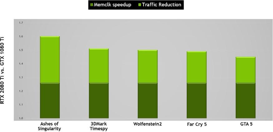
The memory subsystem and compression (traffic reduction) improvements of Turing TU102-based
RTX 2080 Ti deliver approximately 50% effective bandwidth improvements over the Pascal GP102-based 1080 Ti.
Video and Display Engine
Consumer demand for higher resolution displays continues to increase with every passing year. For example, 8K resolution (7680 x 4320) requires four times more pixels than 4K (3820 x 2160). Gamers and hardware enthusiasts also desire displays with higher refresh rates in addition to higher resolution to experience the smoothest possible image.
Turing GPUs include an all-new display engine designed for the new wave of displays, supporting higher resolutions, faster refresh rates, and HDR. Turing supports DisplayPort 1.4a allowing 8K resolution at 60 Hz and includes VESA’s Display Stream Compression (DSC) 1.2 technology, providing higher compression that is visually lossless. Table 2 shows the DisplayPort support in the Turing GPUs.
| Bandwidth/Lane | Max Resolution Supported | |
| DisplayPort 1.2 | 5.4 Gbps | 4K @ 60 Hx |
| DisplayPort 1.3 | 8.1 Gbps | 5K @ 60 Hx |
| DisplayPort 1.4a | 8.1 Gbps | 8K @ 60 Hx |
Turing GPUs can drive two 8K displays at 60 Hz with one cable for each display. 8K resolution can also be sent over USB-C (see USB-C and VirtualLink section below for more details).
Turing’s new display engine supports HDR processing natively in the display pipeline. Tone mapping has also been added to the HDR pipeline. Tone mapping is a technique used to approximate the look of high dynamic range images on standard dynamic range displays. Turing supports the tone mapping formula defined by the ITU-R Recommendation BT.2100 standard to avoid color shift on different HDR displays.
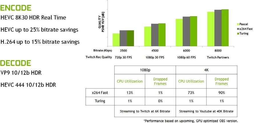
Turing GPUs also ship with an enhanced NVENC encoder unit that adds support for H.265 (HEVC) 8K encode at 30 fps. The new NVENC encoder provides up to 25% bitrate savings for HEVC and up to 15% bitrate savings for H.264.
Turing’s new NVDEC decoder has also been updated to support decoding of HEVC YUV444 10/12b HDR at 30 fps, H.264 8K, and VP9 10/12b HDR.
Turing improves encoding quality compared to prior generation Pascal GPUs and compared to software encoders. Figure 11 shows that on common Twitch and YouTube streaming settings, Turing’s video encoder exceeds the quality of the x264 software-based encoder using the fast encode settings, with dramatically lower CPU utilization. 4K streaming is too heavy a workload for encoding on typical CPU setups, but Turing’s encoder makes 4K streaming possible.
USB-C AND VIRTUALLINK
Supporting VR headsets on today’s PCs requires multiple cables to be connected between the headset and the system; a display cable to send image data from the GPU to the two displays in the headset, a cable to power the headset, and a USB connection to transfer camera streams and read back head pose information from the headset (to update frames rendered by the GPU). The number of cables can be uncomfortable for end users and limit their ability to move around when using the headset. Headset manufacturers need to accommodate the cables, complicating their designs and making them bulkier.
To address this issue, Turing GPUs are designed with hardware support for USB Type-C™ and VirtualLink™. VirtualLink is a new open industry standard that includes leading silicon, software, and headset manufacturers and is led by NVIDIA, Oculus, Valve, Microsoft, and AMD.
VirtualLink has been developed to meet the connectivity requirements of current and next- generation VR headsets. VirtualLink employs a new alternate mode of USB-C, designed to deliver the power, display, and data required to power VR headsets through a single USB-C connector.
VirtualLink simultaneously supports four lanes of High Bit Rate 3 (HBR3) DisplayPort along with the SuperSpeed USB 3 link to the headset for motion tracking. In comparison, USB-C only supports four lanes of HBR3 DisplayPort OR two lanes of HBR3 DisplayPort + two lanes SuperSpeed USB 3.
In addition to easing the setup hassles present in today’s VR headsets, VirtualLink will bring VR to more devices. A single connector solution brings VR to small form factor devices that can accommodate a single, small footprint USB-C connector (such as a thin and light notebook) rather than today’s VR infrastructure which requires a PC that can accommodate multiple connectors.
NVLINK IMPROVES SLI
Prior to the Pascal GPU architecture, NVIDIA GPUs used a single Multiple Input/Output (MIO) interface as the SLI Bridge technology to allow a second (or third or fourth) GPU to transfer its final rendered frame output to the primary GPU that was physically connected to a display. Pascal enhanced the SLI Bridge by using a faster dual-MIO interface, improving bandwidth between the GPUs, allowing higher resolution output, and multiple high-resolution monitors for NVIDIA Surround.
Turing TU102 and TU104 GPUs use NVLink instead of the MIO and PCIe interfaces for SLI GPU-to- GPU data transfers. The Turing TU102 GPU includes two x8 second-generation NVLink links, and Turing TU104 includes one x8 second-generation NVLink link. Each link provides 25 GB/sec peak bandwidth per direction between two GPUs (50 GB/sec bidirectional bandwidth). Two links in TU102 provides 50 GB/sec in each direction, or 100 GB/sec bidirectionally. Two-way SLI is supported with Turing GPUs that have NVLink, but 3-way and 4-way SLI configurations are not supported.
Compared to the previous SLI bridge, the increased bandwidth of the new NVLink bridge enables advanced display topologies that were not previously possible (see Figure 12).
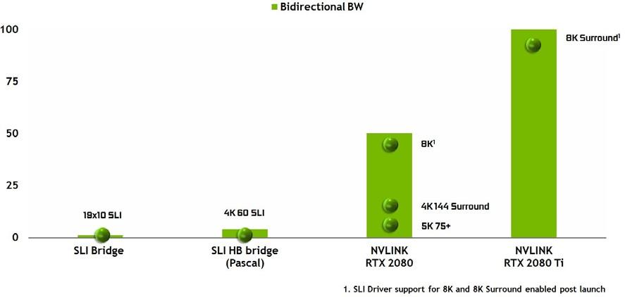
Note: SLI driver support for 8K and 8K Surround will be enabled post-launch.
TURING RAY TRACING TECHNOLOGY
Ray tracing is a computationally-intensive rendering technology that realistically simulates the lighting of a scene and its objects. Turing GPU-based ray tracing technology can render physically correct reflections, refractions, shadows, and indirect lighting in real-time. More details on how ray tracing works can be found in the full Turing White Paper.
In the past, GPU architectures could not perform real time ray-tracing for games or graphical applications using a single GPU. While NVIDIA’s GPU-accelerated NVIDIA Iray® plugins and OptiX ray tracing engine have delivered realistic ray-traced rendering to designers, artists, and technical directors for years, high quality ray tracing effects could not be performed in real-time. Similarly, current NVIDIA Volta GPUs can render realistic movie-quality ray-traced scenes, but not in real- time on a single GPU. Due to its processing intensive nature, ray tracing has not been used in games for any significant rendering tasks. Instead, games that require 30 to 90+ frame/second animations have relied on fast, GPU-accelerated rasterization rendering techniques for years, at the expense of fully realistic looking scenes.
Implementing real-time ray tracing on GPUs was an enormous technical challenge, requiring nearly 10 years of collaboration between NVIDIA’s research, GPU hardware design, and software engineering teams. Real-time ray tracing in games and other applications is made possible by incorporation of multiple new hardware-based ray tracing acceleration engines called RT Cores in Turing TU102, TU104, and TU106 GPUs, combined with NVIDIA RTX software technology.
SOL MAN from NVIDIA SOL ray tracing demo running on a Turing TU102 GPU with NVIDIA RTX technology in real-time is shown in Figure 13 (see demo).
As mentioned, rasterization techniques have been the norm in real-time rendering for years, especially in computer games, and while many rasterized scenes can look very good, rasterization-based rendering has significant limitations. For example, rendering reflections and shadows using only rasterization requires simplifying assumptions that can cause many different types of artifacts. Similarly, static lightmaps may look correct until something moves, rasterized shadows often suffer from aliasing and light leaks, and screen-space reflections can only reflect off objects that are visible on the screen. These artifacts detract from the realism of the gaming experience and are costly for developers and artists to try to fix with additional effects.
Figure 13. SOL MAN from NVIDIA SOL Ray Tracing Demo
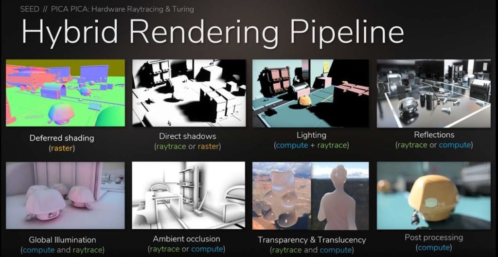
While ray tracing can produce much more realistic imagery than rasterization, it is also computationally intensive. We have found that the best approach is hybrid rendering, a combination of ray tracing and rasterization. With this approach, rasterization is used where it is most effective, and ray tracing is used where it provides the most visual benefit vs rasterization, such as rendering reflections, refractions, and shadows. Figure 14 Shows the hybrid rendering pipeline.
Hybrid Rendering combines ray tracing and rasterization techniques in the rendering pipeline to take advantage of what each does best to render a scene. SEED uses a hybrid rendering model for their PICA PICA real-time ray tracing experiment that features self-learning agents in a procedurally-assembled world. Built using SEED’s R&D engine Halcyon, PICA PICA implements real-time ray tracing using Microsoft DXR and NVIDIA GPUs.
Rasterization and z-buffering is much faster at determining object visibility and can substitute for the primary ray casting stage of the ray tracing process. Ray tracing can then be used for shooting secondary rays to generate high-quality physically correct reflections, refractions, and shadows.
Developers can also use material property thresholds to determine areas to perform ray tracing in a scene. One technique might be to specify that only surfaces with a certain reflectivity level, say 70%, would trigger whether ray tracing should be used on that surface to generate secondary rays.
We expect many developers to use hybrid rasterization/ray tracing techniques to attain high frame rates with excellent image quality. Alternatively, for professional applications where image fidelity is the highest priority, we expect to see use of ray tracing for the entire rendering workload, casting primary and secondary rays to create amazingly realistic rendering.
Turing GPUs not only include dedicated ray tracing acceleration hardware, but also use an advanced acceleration structure described in the next section. Essentially, an entirely new rendering pipeline is available to enable real-time ray tracing in games and other graphics applications using a single Turing GPU (see Figure 15).
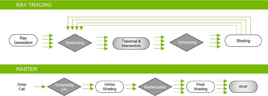
Both Ray tracing and Rasterization pipeline operate simultaneously and cooperatively in Hybrid Rendering model used in Turing GPUs.
While Turing GPUs enable real time ray tracing, the number of primary or secondary rays cast per pixel or surface location varies based on many factors, including scene complexity, resolution, other graphics effects rendered in a scene, and of course GPU horsepower. Do not expect hundreds of rays cast per pixel in real-time. In fact, far fewer rays are needed per pixel when using Turing RT Core acceleration in combination with advanced denoising filtering techniques.
NVIDIA Real-Time Ray Tracing Denoiser modules can significantly reduce the number of rays required per pixel and still produce excellent results.
Real-time ray tracing of selected objects can make many scenes in games and applications look as realistic as high-end movie special effects, or as good as ray-traced images created with professional software-based non-real-time rendering applications. Figure 16 shows an example from the Reflections demo created by Epic Games in collaboration with ILMxLAB and NVIDIA.
Ray-traced reflections, ray-traced area light shadows, and ray-traced ambient occlusion can run on a single Quadro RTX 6000 or GeForce RTX 2080 Ti GPU delivering rendering quality nearly indistinguishable from movies, as this Unreal Engine demo shows.
Figure 16. Unreal Engine Reflections ray tracing demo
Turing ray tracing hardware works with NVIDIA’s RTX ray tracing technology, NVIDIA Real-Time Ray Tracing Libraries, NVIDIA OptiX, the Microsoft DXR API, and the soon-to-come Vulkan ray tracing API. Users will experience real-time, cinematic-quality ray-traced objects and characters in games at playable frame-rates, or visual realism in professional graphics applications that has been impossible with prior GPU architectures in real time.
Turing GPUs can accelerate ray tracing techniques used in many of the following rendering and non-rendering operations:
▶ Reflections and Refractions
▶ Shadows and Ambient Occlusion
▶ Global Illumination
▶ Instant and off-line lightmap baking
▶ Beauty shots and high-quality previews
▶ Primary rays for foveated VR rendering
▶ Occlusion Culling
▶ Physics, Collision Detection, Particle simulations
▶ Audio simulation (ex., NVIDIA VRWorks Audio built on top of the OptiX API)
▶ AI visibility queries
▶ In-engine Path Tracing (non-real-time) to generate reference screenshots for tuning real-time rendering techniques and denoisers, material composition, and scene lighting.
More detail is presented on rendering ray-traced shadows, ambient occlusion, and reflections using Turing ray tracing acceleration in following sections. The NVIDIA Developer Site has more details describing rendering operations that can be accelerated with Turing ray tracing.
TURING RT CORES
At the heart of Turing’s hardware-based ray tracing acceleration is the new RT Core included in each SM. RT Cores accelerate Bounding Volume Hierarchy (BVH) traversal and ray/triangle intersection testing (ray casting) functions. RT Cores perform visibility testing on behalf of threads running in the SM.
RT Cores work together with advanced denoising filtering, a highly-efficient BVH acceleration structure developed by NVIDIA Research, and RTX compatible APIs to achieve real time ray tracing on single Turing GPU. RT Cores traversus the BVH autonomously, and by accelerating traversal and ray/triangle intersection tests, they offload the SM, allowing it to handle other vertex, pixel, and compute shading work. Functions such as BVH building and refitting are handled by the driver, and ray generation and shading is managed by the application through new types of shaders.
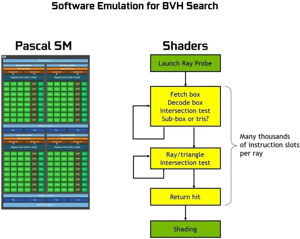
To better understand the function of RT Cores, and what exactly they accelerate, we should first explain how ray tracing is performed on GPUs or CPUs without a dedicated hardware ray tracing engine. Essentially, the process of BVH traversal would need to be performed by shader operations and take thousands of instruction slots per ray cast to test against bounding box intersections in the BVH until finally hitting a triangle and the color at the point of intersection contributes to final pixel color (or if no triangle is hit, background color may be used to shade a pixel).
Ray tracing without hardware acceleration requires thousands of software instruction slots per ray to test successively smaller bounding boxes in the BVH structure until possibly hitting a triangle. It’s a computationally intensive process making it impossible to do on GPUs in real-time without hardware-based ray tracing acceleration (see Figure 17).
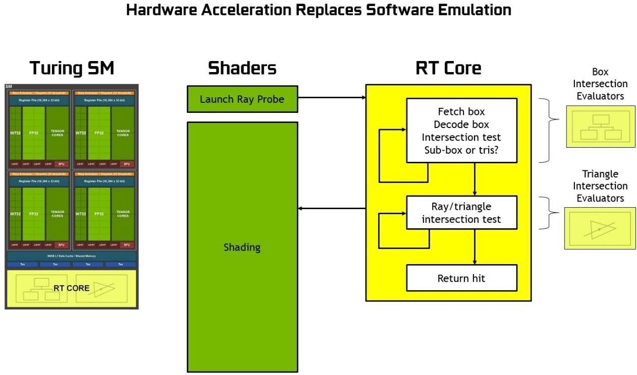
The RT Cores in Turing can process all the BVH traversal and ray-triangle intersection testing, saving the SM from spending the thousands of instruction slots per ray, which could be an enormous amount of instructions for an entire scene. The RT Core includes two specialized units. The first unit does bounding box tests, and the second unit does ray-triangle intersection tests. The SM only has to launch a ray probe, and the RT core does the BVH traversal and ray-triangle tests, and return a hit or no hit to the SM. The SM is largely freed up to do other graphics or compute work. See Figure 18 or an illustration of Turing ray tracing with RT Cores.
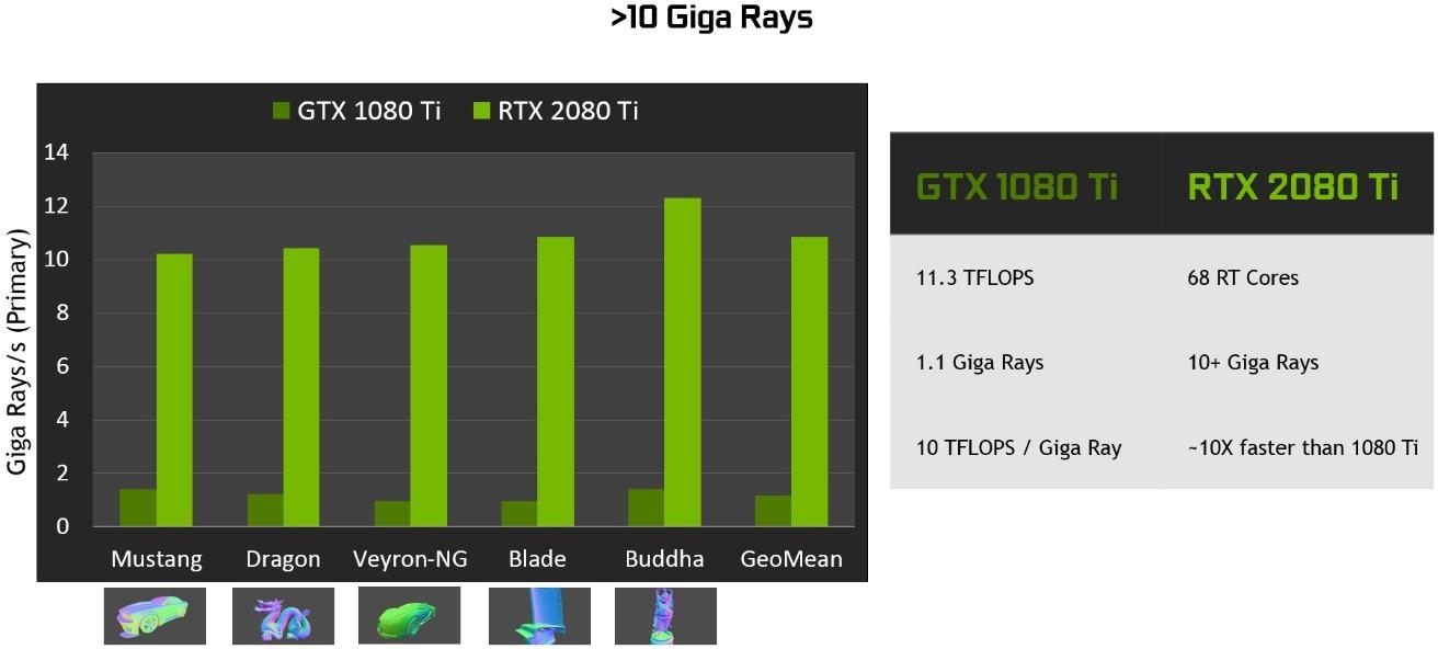
Turing ray tracing performance with RT Cores is significantly faster than ray tracing in Pascal GPUs. Turing can deliver far more Giga Rays/Sec than Pascal on different workloads, as shown in Figure 19. Pascal is spending approximately 1.1 Giga Rays/Sec, or 10 TFLOPS / Giga Ray to do ray tracing in software, whereas Turing can do 10+ Giga Rays/Sec using RT Cores, and run ray tracing 10 times faster.
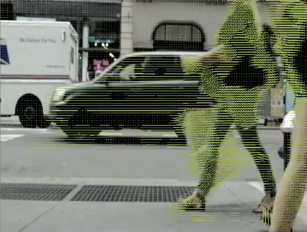
DEEP LEARNING SUPER-SAMPLING (DLSS)
In modern games, rendered frames are not displayed directly, rather they go through a post processing image enhancement step that combines input from multiple rendered frames, trying to remove visual artifacts such as aliasing while preserving detail. For example, Temporal Anti- Aliasing (TAA), a shader-based algorithm that combines two frames using motion vectors to determine where to sample the previous frame, is one of the most common image enhancement algorithms in use today. However, this image enhancement process is fundamentally very difficult to get right.
NVIDIA’s researchers recognized that this type of problem – an image analysis and optimization problem with no clean algorithmic solution – would be a perfect application for AI. As discussed earlier in this document, image processing cases (for example ImageNet) are among the biggest successful applications of deep learning. Deep learning has now achieved super-human ability to recognize dogs, cats, birds etc., from looking at the raw pixels in an image. In this case, the goal would be to combine rendered images, based on looking at raw pixels, to produce a high-quality result—a different objective but using similar capabilities.
The deep neural network (DNN) that was developed to solve this challenge is called Deep Learning Super-Sampling (DLSS). DLSS produces a much higher quality output than TAA from a given set of input samples, and we leverage this capability to improve overall performance.
Whereas TAA renders at the final target resolution and then combines frames, subtracting detail, DLSS allows faster rendering at a lower input sample count, and then infers a result that at target resolution is similar quality to the TAA result, but with half the shading work.
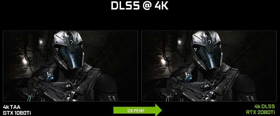
Figure 20, below shows a sampling of results on the UE4 Infiltrator demo. DLSS provides image quality that is similar to TAA, with much improved performance. The much faster raw rendering horsepower of RTX 2080 Ti, combined with the performance uplift from DLSS and Tensor Cores, enables RTX 2080 Ti to achieve 2x the performance of GTX 1080 Ti.
The key to this result is the training process for DLSS, where it gets the opportunity to learn how to produce the desired output based on large numbers of super-high-quality examples. To train the network, we collect thousands of “ground truth” reference images rendered with the gold standard method for perfect image quality, 64x supersampling (64xSS). 64x supersampling means that instead of shading each pixel once, we shade at 64 different offsets within the pixel, and then combine the outputs, producing a resulting image with ideal detail and anti-aliasing quality. We also capture matching raw input images rendered normally. Next, we start training the DLSS network to match the 64xSS output frames, by going through each input, asking DLSS to produce an output, measuring the difference between its output and the 64xSS target, and adjusting the weights in the network based on the differences, through a process called back propagation.
After many iterations, DLSS learns on its own to produce results that closely approximate the quality of 64xSS, while also learning to avoid the problems with blurring, disocclusion, and transparency that affect classical approaches like TAA.
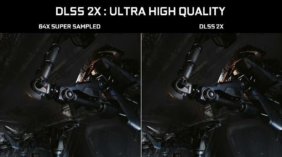
In addition to the DLSS capability described above, which is the standard DLSS mode, we provide a second mode, called DLSS 2X. In this case, DLSS input is rendered at the final target resolution and then combined by a larger DLSS network to produce an output image that approaches the level of the 64x super sample rendering – a result that would be impossible to achieve in real time by any traditional means. Figure 21 shows DLSS 2X mode in operation, providing image quality very close to the reference 64x super-sampled image.
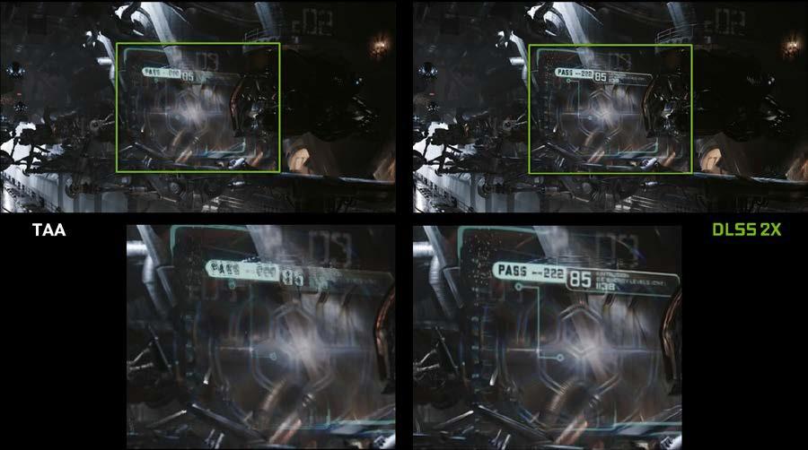
Finally, Figure 22 illustrates one of the challenging cases for multi frame image enhancement. In this case, a semi-transparent screen floats in front of a background that is moving differently. TAA tends to blindly follow the motion vectors of the moving object, blurring the detail on the screen. DLSS is able to recognize that changes in the scene are more complex and combines the inputs in a more intelligent way that avoids the blurring issue.
Conclusion
Graphics has just been reinvented. The new NVIDIA Turing GPU architecture is the most advanced and efficient GPU architecture ever built. Turing implements a new Hybrid Rendering model that combines real-time ray tracing, rasterization, AI, and simulation. Teamed with the next generation graphics APIs, Turing enables massive performance gains and incredibly realistic graphics for PC games and professional applications.
Future blog posts will include more details on Turing’s advanced shader technology. If you wish to dive deeper into the Turing architecture, please download the full NVIDIA Turing Architecture White Paper. You can also find more information on RTX technology on the RTX developer page or read about how to RTX and DirectX 12 ray tracing works here.