Today at the 2017 GPU Technology Conference in San Jose, NVIDIA CEO Jen-Hsun Huang announced the new NVIDIA Tesla V100, the most advanced accelerator ever built.
From recognizing speech to training virtual personal assistants to converse naturally; from detecting lanes on the road to teaching autonomous cars to drive; data scientists are taking on increasingly complex challenges with AI. Solving these kinds of problems requires training exponentially more complex deep learning models in a practical amount of time.
High Performance Computing (HPC) is a fundamental pillar of modern science. From predicting weather, to discovering drugs, to finding new energy sources, researchers use large computing systems to simulate and predict our world. AI extends traditional HPC by allowing researchers to analyze large volumes of data for rapid insights where simulation alone cannot fully predict the real world.
Based on the new NVIDIA Volta GV100 GPU and powered by ground-breaking technologies, Tesla V100 is engineered for the convergence of HPC and AI. It offers a platform for HPC systems to excel at both computational science for scientific simulation and data science for finding insights in data.
In this blog post we will provide an overview of the Volta architecture and its benefits to you as a developer.
Tesla V100: The AI Computing and HPC Powerhouse
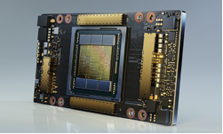
The NVIDIA Tesla V100 accelerator is the world’s highest performing parallel processor, designed to power the most computationally intensive HPC, AI, and graphics workloads.
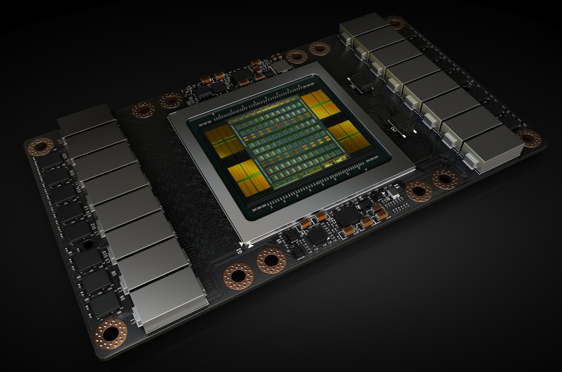
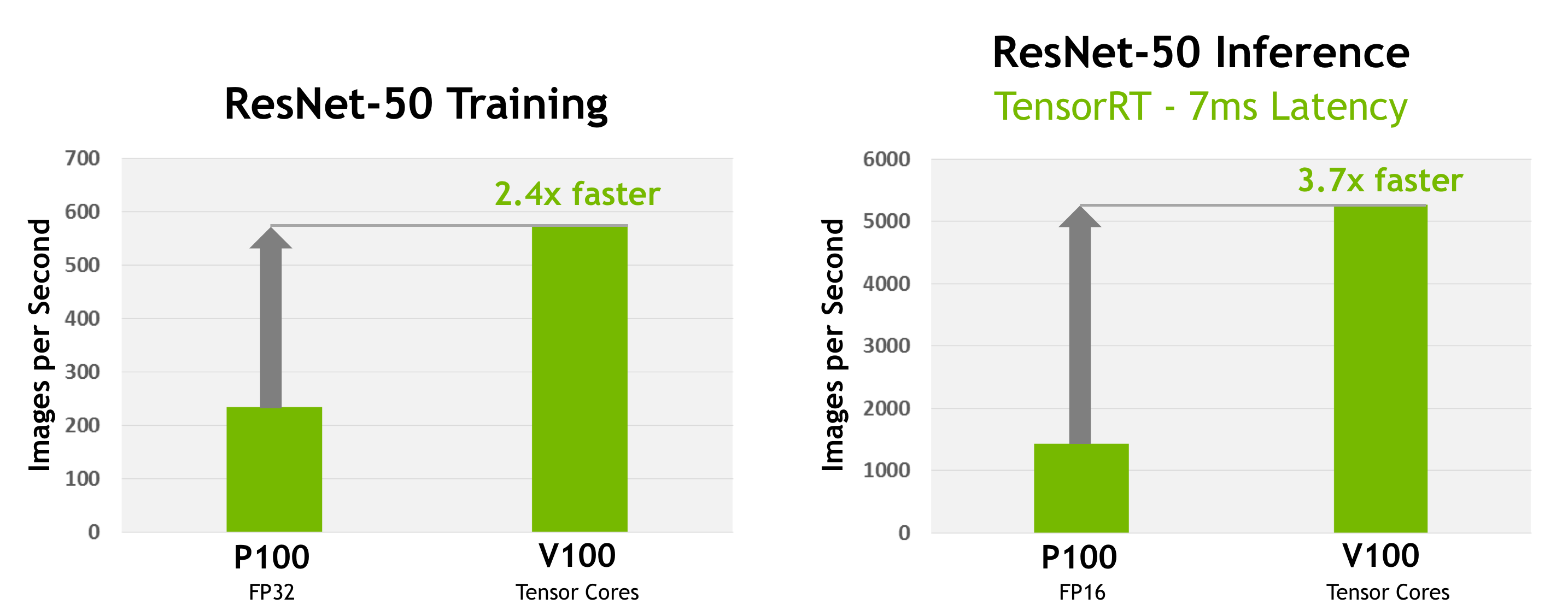
The GV100 GPU includes 21.1 billion transistors with a die size of 815 mm2. It is fabricated on a new TSMC 12 nm FFN high performance manufacturing process customized for NVIDIA. GV100 delivers considerably more compute performance, and adds many new features compared to its predecessor, the Pascal GP100 GPU and its architecture family. Further simplifying GPU programming and application porting, GV100 also improves GPU resource utilization. GV100 is an extremely power-efficient processor, delivering exceptional performance per watt. Figure 2 shows Tesla V100 performance for deep learning training and inference using the ResNet-50 deep neural network.
Key Features
Key compute features of Tesla V100 include the following.
- New Streaming Multiprocessor (SM) Architecture Optimized for Deep Learning Volta features a major new redesign of the SM processor architecture that is at the center of the GPU. The new Volta SM is 50% more energy efficient than the previous generation Pascal design, enabling major boosts in FP32 and FP64 performance in the same power envelope. New Tensor Cores designed specifically for deep learning deliver up to 12x higher peak TFLOPs for training. With independent, parallel integer and floating point datapaths, the Volta SM is also much more efficient on workloads with a mix of computation and addressing calculations. Volta’s new independent thread scheduling capability enables finer-grain synchronization and cooperation between parallel threads. Finally, a new combined L1 Data Cache and Shared Memory subsystem significantly improves performance while also simplifying programming.
- Second-Generation NVLink™ The second generation of NVIDIA’s NVLink high-speed interconnect delivers higher bandwidth, more links, and improved scalability for multi-GPU and multi-GPU/CPU system configurations. GV100 supports up to 6 NVLink links at 25 GB/s for a total of 300 GB/s. NVLink now supports CPU mastering and cache coherence capabilities with IBM Power 9 CPU-based servers. The new NVIDIA DGX-1 with V100 AI supercomputer uses NVLink to deliver greater scalability for ultra-fast deep learning training.
- HBM2 Memory: Faster, Higher Efficiency Volta’s highly tuned 16GB HBM2 memory subsystem delivers 900 GB/sec peak memory bandwidth. The combination of both a new generation HBM2 memory from Samsung, and a new generation memory controller in Volta, provides 1.5x delivered memory bandwidth versus Pascal GP100 and greater than 95% memory bandwidth efficiency running many workloads.
- Volta Multi-Process Service Volta Multi-Process Service (MPS) is a new feature of the Volta GV100 architecture providing hardware acceleration of critical components of the CUDA MPS server, enabling improved performance, isolation, and better quality of service (QoS) for multiple compute applications sharing the GPU. Volta MPS also triples the maximum number of MPS clients from 16 on Pascal to 48 on Volta.
- Enhanced Unified Memory and Address Translation Services GV100 Unified Memory technology in Volta GV100 includes new access counters to allow more accurate migration of memory pages to the processor that accesses the pages most frequently, improving efficiency for accessing memory ranges shared between processors. On IBM Power platforms, new Address Translation Services (ATS) support allows the GPU to access the CPU’s page tables directly.
- Cooperative Groups and New Cooperative Launch APIs Cooperative Groups is a new programming model introduced in CUDA 9 for organizing groups of communicating threads. Cooperative Groups allows developers to express the granularity at which threads are communicating, helping them to express richer, more efficient parallel decompositions. Basic Cooperative Groups functionality is supported on all NVIDIA GPUs since Kepler. Pascal and Volta include support for new Cooperative Launch APIs that support synchronization amongst CUDA thread blocks. Volta adds support for new synchronization patterns.
- Maximum Performance and Maximum Efficiency Modes In Maximum Performance mode, the Tesla V100 accelerator will operate unconstrained up to its TDP (Thermal Design Power) level of 300W to accelerate applications that require the fastest computational speed and highest data throughput. Maximum Efficiency Mode allows data center managers to tune power usage of their Tesla V100 accelerators to operate with optimal performance per watt. A not-to-exceed power cap can be set across all GPUs in a rack, reducing power consumption dramatically, while still obtaining excellent rack performance.
- Volta Optimized Software New versions of deep learning frameworks such as Caffe2, MXNet, CNTK, TensorFlow, and others harness the performance of Volta to deliver dramatically faster training times and higher multi-node training performance. Volta-optimized versions of GPU accelerated libraries such as cuDNN, cuBLAS, and TensorRT leverage the new features of the Volta GV100 architecture to deliver higher performance for both deep learning and High Performance Computing (HPC) applications. The NVIDIA CUDA Toolkit version 9.0 includes new APIs and support for Volta features to provide even easier programmability.
GV100 GPU Hardware Architecture
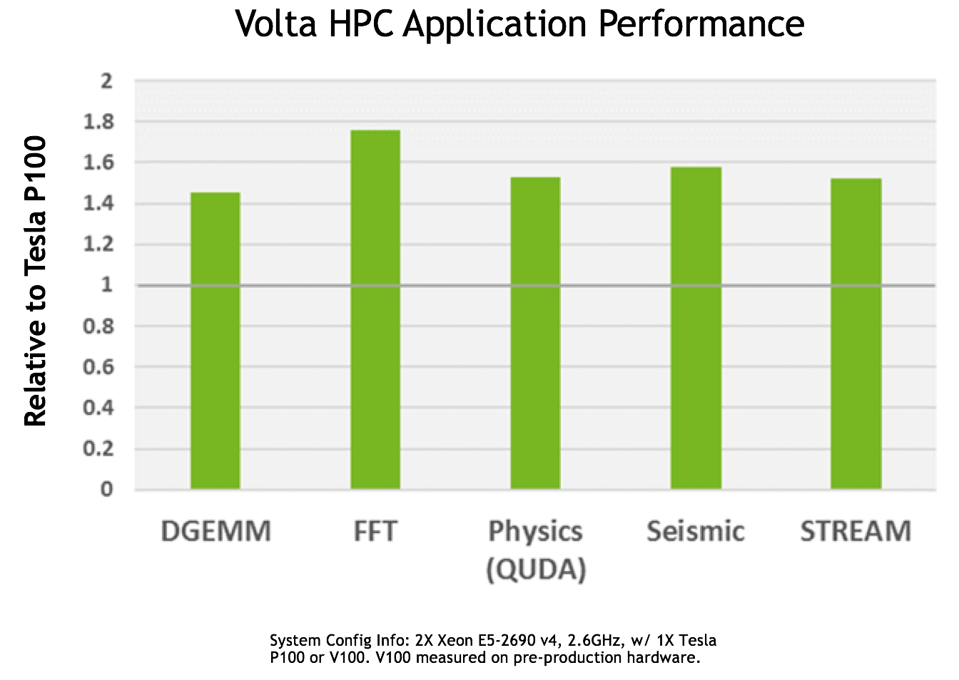
The NVIDIA Tesla V100 accelerator featuring the Volta GV100 GPU is the highest performing parallel computing processor in the world today. GV100 has significant new hardware innovations that provide tremendous speedups for deep learning algorithms and frameworks, in addition to providing far more computational horsepower for HPC systems and applications, as Figure 3 shows.
Tesla V100 delivers industry-leading floating-point and integer performance. Peak computation rates (based on GPU Boost clock rate) are:
- 7.8 TFLOP/s of double precision floating-point (FP64) performance;
- 15.7 TFLOP/s of single precision (FP32) performance;
- 125 Tensor TFLOP/s of mixed-precision matrix-multiply-and-accumulate.
Similar to the previous generation Pascal GP100 GPU, the GV100 GPU is composed of multiple Graphics Processing Clusters (GPCs), Texture Processing Clusters (TPCs), Streaming Multiprocessors (SMs), and memory controllers. A full GV100 GPU consists of six GPCs, 84 Volta SMs, 42 TPCs (each including two SMs), and eight 512-bit memory controllers (4096 bits total). Each SM has 64 FP32 Cores, 64 INT32 Cores, 32 FP64 Cores, and 8 new Tensor Cores. Each SM also includes four texture units.
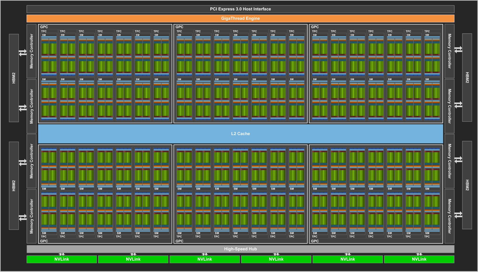
With 84 SMs, a full GV100 GPU has a total of 5376 FP32 cores, 5376 INT32 cores, 2688 FP64 cores, 672 Tensor Cores, and 336 texture units. Each memory controller is attached to 768 KB of L2 cache, and each HBM2 DRAM stack is controlled by a pair of memory controllers. The full GV100 GPU includes a total of 6144 KB of L2 cache. Figure 4 shows a full GV100 GPU with 84 SMs (different products can use different configurations of GV100). The Tesla V100 accelerator uses 80 SMs.
Table 1 compares Tesla accelerators over the past 5 years.
| Tesla Product | Tesla K40 | Tesla M40 | Tesla P100 | Tesla V100 |
|---|---|---|---|---|
| GPU | GK180 (Kepler) | GM200 (Maxwell) | GP100 (Pascal) | GV100 (Volta) |
| SMs | 15 | 24 | 56 | 80 |
| TPCs | 15 | 24 | 28 | 40 |
| FP32 Cores / SM | 192 | 128 | 64 | 64 |
| FP32 Cores / GPU | 2880 | 3072 | 3584 | 5120 |
| FP64 Cores / SM | 64 | 4 | 32 | 32 |
| FP64 Cores / GPU | 960 | 96 | 1792 | 2560 |
| Tensor Cores / SM | NA | NA | NA | 8 |
| Tensor Cores / GPU | NA | NA | NA | 640 |
| GPU Boost Clock | 810/875 MHz | 1114 MHz | 1480 MHz | 1530 MHz |
| Peak FP32 TFLOP/s* | 5.04 | 6.8 | 10.6 | 15.7 |
| Peak FP64 TFLOP/s* | 1.68 | .21 | 5.3 | 7.8 |
| Peak Tensor Core TFLOP/s* | NA | NA | NA | 125 |
| Texture Units | 240 | 192 | 224 | 320 |
| Memory Interface | 384-bit GDDR5 | 384-bit GDDR5 | 4096-bit HBM2 | 4096-bit HBM2 |
| Memory Size | Up to 12 GB | Up to 24 GB | 16 GB | 16 GB |
| L2 Cache Size | 1536 KB | 3072 KB | 4096 KB | 6144 KB |
| Shared Memory Size / SM | 16 KB/32 KB/48 KB | 96 KB | 64 KB | Configurable up to 96 KB |
| Register File Size / SM | 256 KB | 256 KB | 256 KB | 256KB |
| Register File Size / GPU | 3840 KB | 6144 KB | 14336 KB | 20480 KB |
| TDP | 235 Watts | 250 Watts | 300 Watts | 300 Watts |
| Transistors | 7.1 billion | 8 billion | 15.3 billion | 21.1 billion |
| GPU Die Size | 551 mm² | 601 mm² | 610 mm² | 815 mm² |
| Manufacturing Process | 28 nm | 28 nm | 16 nm FinFET+ | 12 nm FFN |
Volta SM (Streaming Multiprocessor)
Architected to deliver higher performance, the Volta SM has lower instruction and cache latencies than past SM designs and includes new features to accelerate deep learning applications.
Major Features include:
- New mixed-precision FP16/FP32 Tensor Cores purpose-built for deep learning matrix arithmetic;
- Enhanced L1 data cache for higher performance and lower latency;
- Streamlined instruction set for simpler decoding and reduced instruction latencies;
- Higher clocks and higher power efficiency.
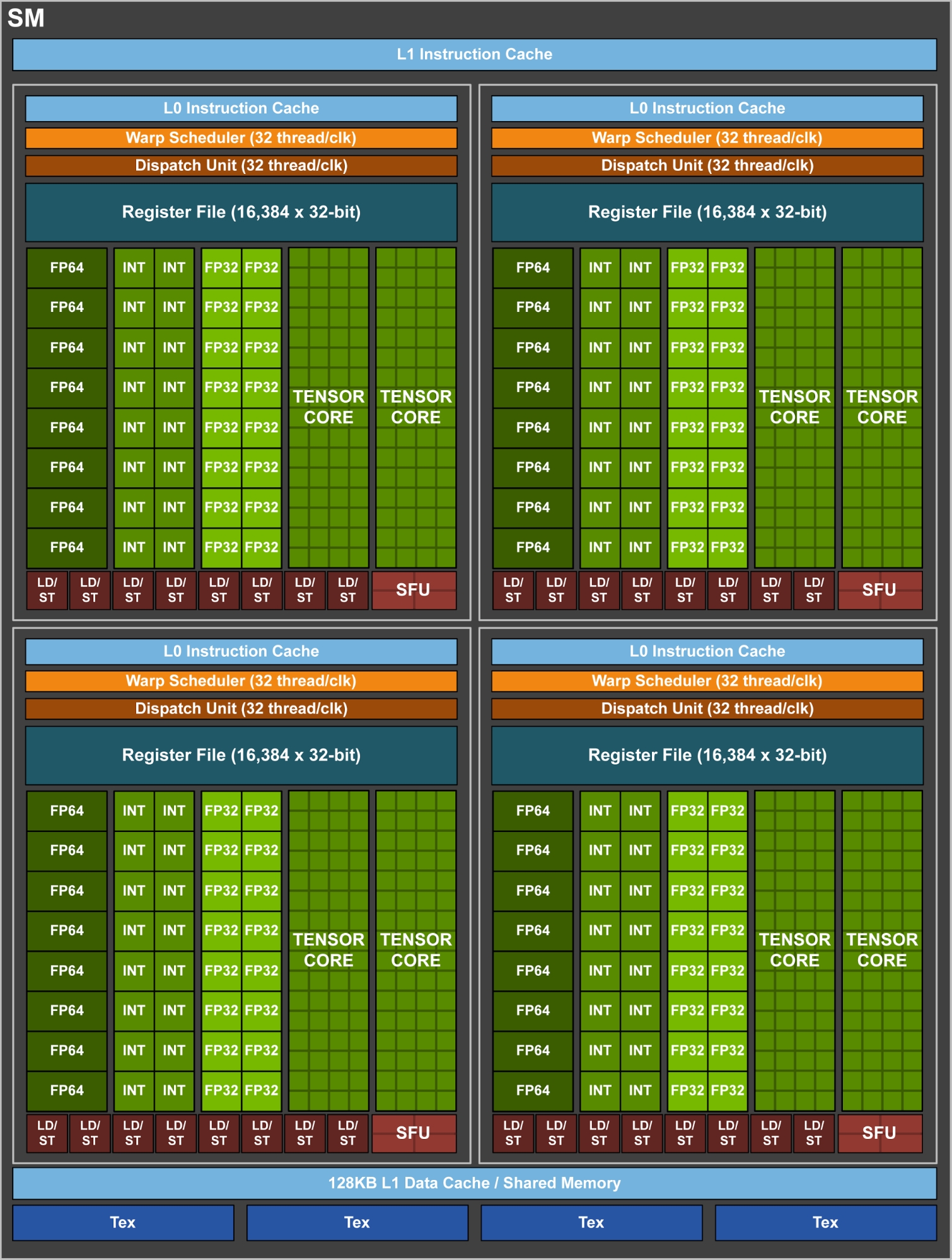
Similar to Pascal GP100, the GV100 SM incorporates 64 FP32 cores and 32 FP64 cores per SM. However, the GV100 SM uses a new partitioning method to improve SM utilization and overall performance. Recall the GP100 SM is partitioned into two processing blocks, each with 32 FP32 Cores, 16 FP64 Cores, an instruction buffer, one warp scheduler, two dispatch units, and a 128 KB Register File. The GV100 SM is partitioned into four processing blocks, each with 16 FP32 Cores, 8 FP64 Cores, 16 INT32 Cores, two of the new mixed-precision Tensor Cores for deep learning matrix arithmetic, a new L0 instruction cache, one warp scheduler, one dispatch unit, and a 64 KB Register File. Note that the new L0 instruction cache is now used in each partition to provide higher efficiency than the instruction buffers used in prior NVIDIA GPUs. (See the Volta SM in Figure 5).
While a GV100 SM has the same number of registers as a Pascal GP100 SM, the entire GV100 GPU has far more SMs, and thus many more registers overall. In aggregate, GV100 supports more threads, warps, and thread blocks in flight compared to prior GPU generations.
Overall shared memory across the entire GV100 GPU is increased due to the increased SM count and potential for up to 96 KB of Shared Memory per SM, compared to 64 KB in GP100.
Unlike Pascal GPUs, which could not execute FP32 and INT32 instructions simultaneously, the Volta GV100 SM includes separate FP32 and INT32 cores, allowing simultaneous execution of FP32 and INT32 operations at full throughput, while also increasing instruction issue throughput. Dependent instruction issue latency is also reduced for core FMA math operations, requiring only four clock cycles on Volta, compared to six cycles on Pascal.
Tensor Cores
Tesla P100 delivered considerably higher performance for training neural networks compared to the prior generation NVIDIA Maxwell and Kepler architectures, but the complexity and size of neural networks have continued to grow. New networks that have thousands of layers and millions of neurons demand even higher performance and faster training times.
New Tensor Cores are the most important feature of the Volta GV100 architecture to help deliver the performance required to train large neural networks. Tesla V100’s Tensor Cores deliver up to 125 Tensor TFLOPS for training and inference applications. Tensor Cores provide up to 12x higher peak TFLOPS on Tesla V100 for deep learning training compared to P100 FP32 operations, and for deep learning inference, up to 6x higher peak TFLOPS compared to P100 FP16 operations. The Tesla V100 GPU contains 640 Tensor Cores: 8 per SM.
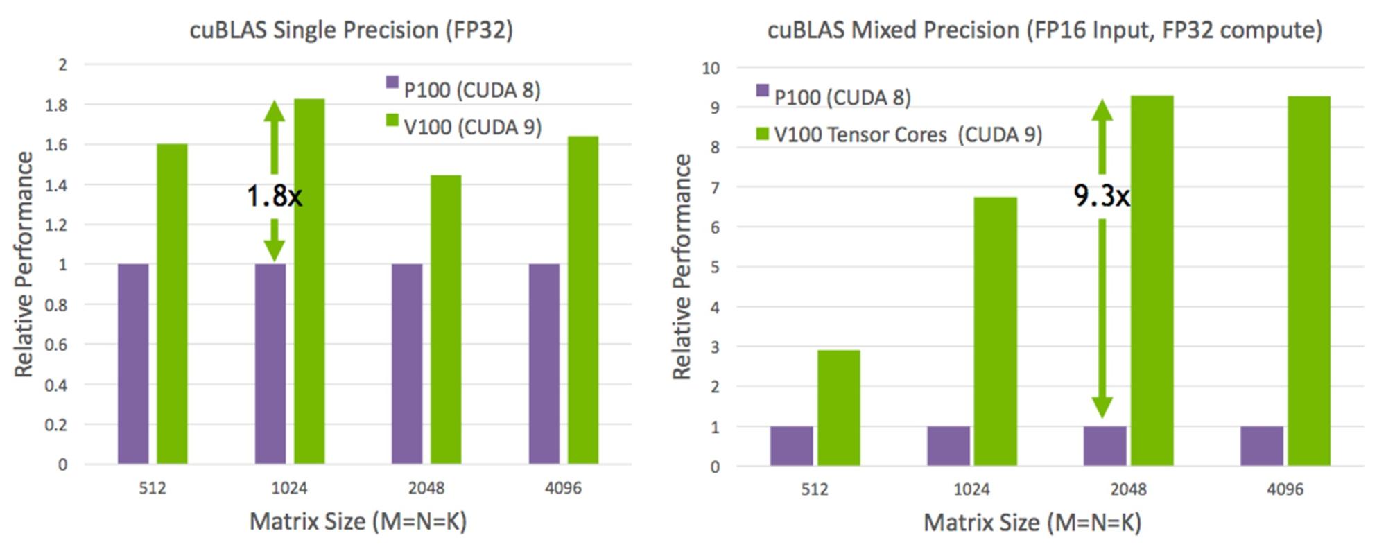
Matrix-Matrix multiplication (BLAS GEMM) operations are at the core of neural network training and inferencing, and are used to multiply large matrices of input data and weights in the connected layers of the network. As Figure 6 shows, Tensor Cores in the Tesla V100 GPU boost the performance of these operations by more than 9x compared to the Pascal-based GP100 GPU.
Tensor Cores and their associated data paths are custom-crafted to dramatically increase floating-point compute throughput at only modest area and power costs. Clock gating is used extensively to maximize power savings.
Each Tensor Core provides a 4x4x4 matrix processing array which performs the operation 


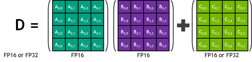
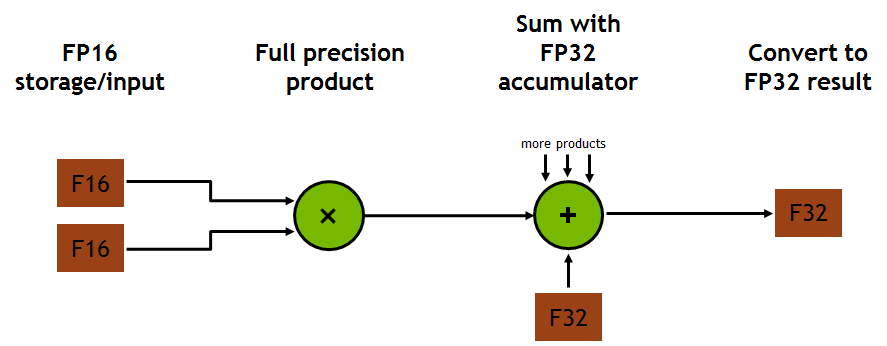
Each Tensor Core performs 64 floating point FMA mixed-precision operations per clock (FP16 input multiply with full-precision product and FP32 accumulate, as Figure 8 shows) and 8 Tensor Cores in an SM perform a total of 1024 floating point operations per clock. This is a dramatic 8X increase in throughput for deep learning applications per SM compared to Pascal GP100 using standard FP32 operations, resulting in a total 12X increase in throughput for the Volta V100 GPU compared to the Pascal P100 GPU. Tensor Cores operate on FP16 input data with FP32 accumulation. The FP16 multiply results in a full precision result that is accumulated in FP32 operations with the other products in a given dot product for a 4x4x4 matrix multiply, as Figure 8 shows.
During program execution, multiple Tensor Cores are used concurrently by a full warp of execution. The threads within a warp provide a larger 16x16x16 matrix operation to be processed by the Tensor Cores. CUDA exposes these operations as Warp-Level Matrix Operations in the CUDA C++ API. These C++ interfaces provide specialized matrix load, matrix multiply and accumulate, and matrix store operations to efficiently utilize Tensor Cores in CUDA C++ programs.
In addition to CUDA C++ interfaces to program Tensor Cores directly, CUDA 9 cuBLAS and cuDNN libraries include new library interfaces to make use of Tensor Cores for deep learning applications and frameworks. NVIDIA has worked with many popular deep learning frameworks such as Caffe2 and MXNet to enable the use of Tensor Cores for deep learning research on Volta GPU based systems. NVIDIA continues to work with other framework developers to enable broad access to Tensor Cores for the entire deep learning ecosystem.
Enhanced L1 Data Cache and Shared Memory
The new combined L1 data cache and shared memory subsystem of the Volta SM significantly improves performance while also simplifying programming and reducing the tuning required to attain at or near-peak application performance.
Combining data cache and shared memory functionality into a single memory block provides the best overall performance for both types of memory accesses. The combined capacity is 128 KB/SM, more than 7 times larger than the GP100 data cache, and all of it is usable as a cache by programs that do not use shared memory. Texture units also use the cache. For example, if shared memory is configured to 64 KB, texture and load/store operations can use the remaining 64 KB of L1.
Integration within the shared memory block ensures the Volta GV100 L1 cache has much lower latency and higher bandwidth than the L1 caches in past NVIDIA GPUs. The L1 In Volta functions as a high-throughput conduit for streaming data while simultaneously providing high-bandwidth and low-latency access to frequently reused data—the best of both worlds. This combination is unique to Volta and delivers more accessible performance than in the past.

A key reason to merge the L1 data cache with shared memory in GV100 is to allow L1 cache operations to attain the benefits of shared memory performance. Shared memory provides high bandwidth and low latency, but the CUDA programmer needs to explicitly manage this memory. Volta narrows the gap between applications that explicitly manage shared memory and those that access data in device memory directly. To demonstrate this, we modified a suite of programs by replacing shared memory arrays with device memory arrays so that accesses would go through L1 cache. As Figure 9 shows, on Volta these codes saw only a 7% performance loss running without using shared memory, compared to a 30% performance loss on Pascal. While shared memory remains the best choice for maximum performance, the new Volta L1 design enables programmers to get excellent performance quickly, with less programming effort.
Compute Capability
The GV100 GPU supports the new Compute Capability 7.0. Table 2 compares the parameters of different Compute Capabilities for NVIDIA GPU architectures.
| GPU | Kepler GK180 | Maxwell GM200 | Pascal GP100 | Volta GV100 |
|---|---|---|---|---|
| Compute Capability | 3.5 | 5.2 | 6.0 | 7.0 |
| Threads / Warp | 32 | 32 | 32 | 32 |
| Max Warps / SM | 64 | 64 | 64 | 64 |
| Max Threads / SM | 2048 | 2048 | 2048 | 2048 |
| Max Thread Blocks / SM | 16 | 32 | 32 | 32 |
| Max 32-bit Registers / SM | 65536 | 65536 | 65536 | 65536 |
| Max Registers / Block | 65536 | 32768 | 65536 | 65536 |
| Max Registers / Thread | 255 | 255 | 255 | 255* |
| Max Thread Block Size | 1024 | 1024 | 1024 | 1024 |
| FP32 Cores / SM | 192 | 128 | 64 | 64 |
| # of Registers to FP32 Cores Ratio | 341 | 512 | 1024 | 1024 |
| Shared Memory Size / SM | 16 KB/32 KB/48 KB | 96 KB | 64 KB | Configurable up to 96 KB |
Independent Thread Scheduling
The Volta architecture is designed to be significantly easier to program than prior GPUs, enabling users to work productively on more complex and diverse applications. Volta GV100 is the first GPU to support independent thread scheduling, which enables finer-grain synchronization and cooperation between parallel threads in a program. One of the major design goals for Volta was to reduce the effort required to get programs running on the GPU, and to enable greater flexibility in thread cooperation, leading to higher efficiency for fine-grained parallel algorithms.
Prior NVIDIA GPU SIMT Models
Pascal and earlier NVIDIA GPUs execute groups of 32 threads—known as warps—in SIMT (Single Instruction, Multiple Thread) fashion. The Pascal warp uses a single program counter shared amongst all 32 threads, combined with an “active mask” that specifies which threads of the warp are active at any given time. This means that divergent execution paths leave some threads inactive, serializing execution for different portions of the warp as Figure 10 shows. The original mask is stored until the warp reconverges at the end of the divergent section, at which point the mask is restored and the threads run together once again.
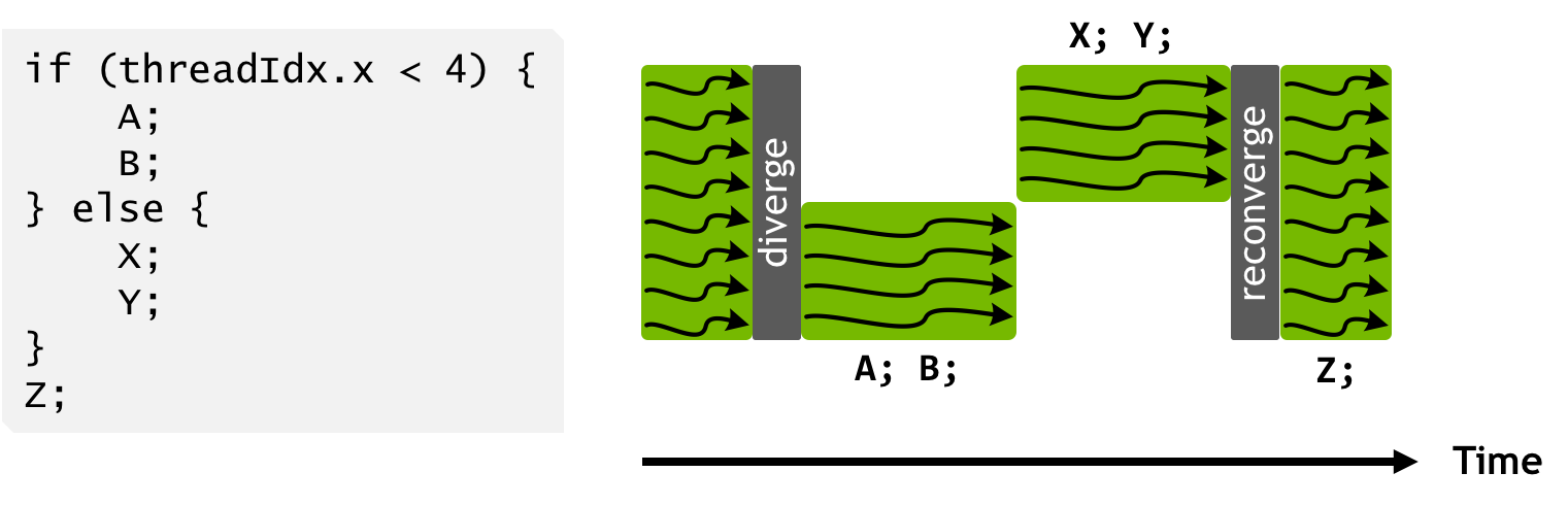
The Pascal SIMT execution model maximizes efficiency by reducing the quantity of resources required to track thread state and by aggressively reconverging threads to maximize parallelism. Tracking thread state in aggregate for the whole warp, however, means that when the execution pathway diverges, the threads which take different branches lose concurrency until they reconverge. This loss of concurrency means that threads from the same warp in divergent regions or different states of execution cannot signal each other or exchange data. This presents an inconsistency in which threads from different warps continue to run concurrently, but diverged threads from the same warp run sequentially until they reconverge. This means, for example, that algorithms requiring fine-grained sharing of data guarded by locks or mutexes can easily lead to deadlock, depending on which warp the contending threads come from. Therefore, on Pascal and earlier GPUs, programmers have to avoid fine-grained synchronization or rely on lock-free or warp-aware algorithms.
Volta SIMT Model
Volta transforms this picture by enabling equal concurrency between all threads, regardless of warp. It does this by maintaining execution state per thread, including the program counter and call stack, as Figure 11 shows.
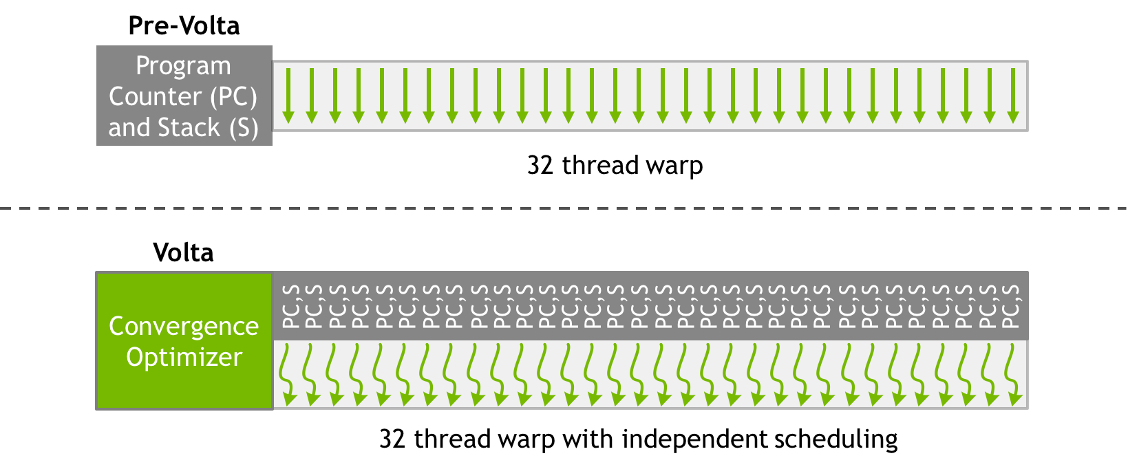
Volta’s independent thread scheduling allows the GPU to yield execution of any thread, either to make better use of execution resources or to allow one thread to wait for data to be produced by another. To maximize parallel efficiency, Volta includes a schedule optimizer which determines how to group active threads from the same warp together into SIMT units. This retains the high throughput of SIMT execution as in prior NVIDIA GPUs, but with much more flexibility: threads can now diverge and reconverge at sub-warp granularity, and Volta will still group together threads which are executing the same code and run them in parallel.
Execution of the code example from Figure 10 looks somewhat different on Volta. Statements from the if and else branches in the program can now be interleaved in time as Figure 12 shows. Note that execution is still SIMT: at any given clock cycle CUDA cores execute the same instruction for all active threads in a warp just as before, retaining the execution efficiency of previous architectures. Importantly, Volta’s ability to independently schedule threads within a warp makes it possible to implement complex, fine-grained algorithms and data structures in a more natural way. While the scheduler supports independent execution of threads, it optimizes non-synchronizing code to maintain as much convergence as possible for maximum SIMT efficiency.
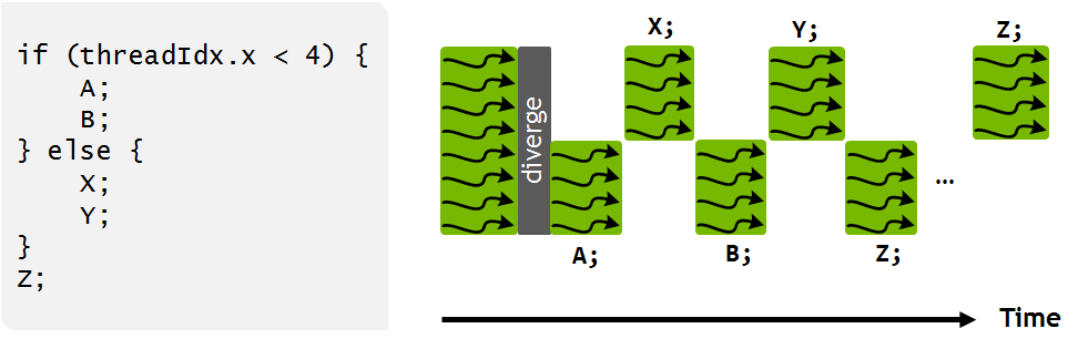
It is interesting to note that Figure 12 does not show execution of statement Z by all threads in the warp at the same time. This is because the scheduler must conservatively assume that Z may produce data required by other divergent branches of execution in which case it would be unsafe to automatically enforce reconvergence. In the common case where A, B, X, and Y do not consist of synchronizing operations, the scheduler can identify that it is safe for the warp to naturally reconverge on Z, as on prior architectures.
Programs can call the new CUDA 9 warp synchronization function __syncwarp() to force reconvergence, as Figure 13 shows. In this case, the divergent portions of the warp might not execute Z together, but all execution pathways from threads within a warp will complete before any thread reaches the statement after the __syncwarp(). Similarly, placing the call to __syncwarp() before the execution of Z would force reconvergence before executing Z, potentially enabling greater SIMT efficiency if the developer knows that this is safe for their application.

Starvation-Free Algorithms
Starvation-free algorithms are a key pattern enabled by independent thread scheduling. These are concurrent computing algorithms that are guaranteed to execute correctly so long as the system ensures that all threads have adequate access to a contended resource. For example, a mutex (or lock) may be used in a starvation-free algorithm if a thread attempting to acquire the mutex is guaranteed eventually to succeed. In a system that does not support starvation-freedom, one or more threads may repeatedly acquire and release a mutex while starving another thread from ever successfully acquiring the mutex.
Consider a simplified example that Volta’s independent thread scheduling enables: inserting nodes into a doubly-linked list in a multithreaded application.
__device__ void insert_after(Node *a, Node *b)
{
    Node *c;
    lock(a); lock(a->next);
    c = a->next;

    a->next = b;
    b->prev = a;

    b->next = c;
    c->prev = b;

    unlock(c); unlock(a);
}
In this example, each element of a doubly linked list has at least three components: a next pointer, a previous pointer, and a lock providing the owner exclusive access to update the node. Figure 14 shows the insertion of node B after node A with updates to the next and previous pointers of A and C.

Independent thread scheduling in Volta ensures that even if a thread T0 currently holds the lock for node A, another thread T1 in the same warp can successfully wait for the lock to become available without impeding the progress of thread T0. Note, however, that because active threads in a warp execute together, threads spinning on a lock may degrade the performance of the thread holding the lock.
It is also important to note that the use of a per-node lock in the above example is critical for performance on the GPU. Traditional doubly-linked list implementations may use a coarse-grained lock that provides exclusive access to the entire structure, rather than separately protecting individual nodes. This approach typically leads to poor performance in applications with many threads—Volta may have up to 163,840 concurrent threads—caused by extremely high contention for the lock. By using a fine-grained lock on each node, the average per-node contention in large lists will usually be low except under certain pathological node insertion patterns.
This doubly-linked list with fine-grained locks is a simple example, but it demonstrates how independent thread scheduling gives developers the capability to implement familiar algorithms and data structures on the GPU in a natural way.
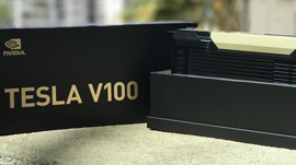
NVIDIA Tesla V100: The World’s Most Advanced Data Center GPU
NVIDIA® Tesla® V100 is the world’s most advanced data center GPU ever built to accelerate AI, HPC, and Graphics. Powered by the latest GPU architecture, NVIDIA Volta™, Tesla V100 offers the performance of 100 CPUs in a single GPU—enabling data scientists, researchers, and engineers to tackle challenges that were once impossible.
With 640 Tensor cores, Tesla V100 is the world’s first GPU to break the 100 TFLOPS barrier of deep learning performance. The next generation of NVIDIA® NVLink™ connects multiple V100 GPUs at up to 300 GB/s to create the world’s most powerful computing servers. AI models that would consume weeks of computing resources can now be trained in a few days. With this dramatic reduction in training time, a whole new world of problems will now be solvable with AI.
Download the Tesla V100 White Paper Today!
 The new Tesla V100 architecture white paper provides detailed coverage of the Volta architecture, the Tesla V100 accelerator, deep learning, and the NVIDIA DGX-1 with Tesla V100, the new NVIDIA DGX Station personal AI supercomputer, and more.
Acknowledgements
We would like to thank Sridhar Ramaswamy, Stephen Jones, Jonah Alben and many NVIDIA architects and engineers for contributing to this post.